- 您现在的位置:买卖IC网 > Sheet目录409 > DR-TRC103-950-DK (RFM)KIT DEV 950MHZ RFIC SRR
�� �
�
�If� FSK� is� selected,� the� demodulation� is� performed� by� analyzing� the� phase� between� the� I� and� Q� limited� signals� at�
�the� output� of� the� base-band� channels.�
�If� OOK� is� selected,� the� demodulation� is� performed� by� comparing� the� RSSI� output� value� stored� in� RXCFG14_�
�RSSI[7..0]� register� to� the� threshold� which� can� be� either� a� fixed� value� or� a� time-variant� value� depending� on� the�
�past� history� of� the� RSSI� output.� Table� 7� gives� the� three� main� possible� procedures,� which� can� be� selected� via� the�
�register� MCFG01_RX_OOK[4..3]� :�
�OOK� Mode�
�Fixed� Threshold�
�Peak�
�Average�
�MCFG01_RX_OOK[4..3]�
�00�
�01�
�10�
�Description�
�RSSI� output� is� compared� with� a� fixed� threshold� stored� in�
�MCFG04_OOK_thresh�
�RSSI� output� is� compared� with� a� threshold� which� is� at� a� fixed�
�offset� below� the� maximum� RSSI.�
�RSSI� output� is� compared� with� the� average� of� the� last� RSSI� values.�
�Table� 7�
�If� the� end-user� application� requires� direct� access� to� the� output� of� the� demodulator,� then� the� RXCFG12_�
�DCLK_Dis[6]� bit� is� set� to� 1� disabling� the� clock� recovery.� In� this� case� the� demodulator� output� is� directly� connected�
�to� the� DATA� pin� and� the� IRQ1� pin� (DCLK)� is� set� to� low.�
�For� proper� operation� of� the� TRC103� demodulator� in� FSK� mode,� the� modulation� index� β� of� the� input� signal� should�
�meet� the� following� condition:�
�β� =�
�2*F� DEV�
�≥� 2�
�BR�
�where� F� DEV� is� the� frequency� deviation� in� hertz� (Hz)� and� BR� is� the� data� rate� in� bits� per� second� (b/s).�
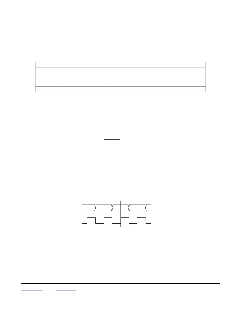
�3.2� Continuous� Mode� Data� and� Clock� Recovery�
�The� raw� output� signal� from� the� demodulator� may� contain� jitter� and� glitches.� Data� and� clock� recovery� converts� the�
�data� output� of� the� demodulator� into� a� glitch-free� bit-stream� DATA� and� generates� a� synchronized� clock� DCLK� to� be�
�used� for� sampling� the� DATA� output� as� shown� in� Figure� 8.� DCLK� is� available� on� pin� IRQ1� when� the� TRC103� oper-�
�ates� in� continuous� mode.�
�D� a� ta� &�
�C� lo� c� k� R� e� c� o� v� e� r� y� T� im� in� g�
�D� A� T� A�
�D� C� L� K�
�D� A� T� A� v� a� lid� o� n� r� is� in� g� e� d� g� e� o� f� D� C� L� K�
�Figure� 8�
�To� ensure� correct� operation� of� the� data� and� clock� recovery� circuit,� the� following� conditions� have� to� be� satisfied:�
�?�
�?�
�?�
�A� 1-0-1-0…� preamble� of� at� least� 24� bits� is� required� for� synchronization�
�The� transmitted� bit� stream� must� have� at� least� one� transition� from� 0� to� 1� or� from� 1� to� 0� every� 8� bits� during�
�transmission�
�The� bit� rate� accuracy� must� be� better� than� 2� %.�
�www.RFM.com� E-mail:� info@rfm.com�
�?� 2009-2010� by� RF� Monolithics,� Inc.�
�Technical� support� +1.800.704.6079�
�Page� 13� of� 65�
�TRC103� -� 11/29/12�
�发布紧急采购,3分钟左右您将得到回复。
相关PDF资料
DR-TRC105-372-DK
DEV KIT TRC105
DR-TRC105-450-EV
BOARD EVALUATION 450MHZ RFM RFIC
DR-TXC100-433
BOARD EVALUATION 433MHZ TXC100
DR-WLS1273L-EV
KIT EVAL FOR WLS1273L
DR7000-DK
3G DEVELOPMENT KIT 433.92MHZ
DR7001-DK
3G DEVELOPMENT KIT 315 MHZ
DR7003-DK
3G DEVELOPMENT KIT 303.825 MHZ
DR8000-DK
3G DEVELOPMENT KIT 916MHZ
相关代理商/技术参数
DR-TRC103-950-EV
功能描述:BOARD EVALUATION 950MHZ RFM RFIC RoHS:否 类别:RF/IF 和 RFID >> RF 评估和开发套件,板 系列:- 标准包装:1 系列:- 类型:GPS 接收器 频率:1575MHz 适用于相关产品:- 已供物品:模块 其它名称:SER3796
DR-TRC104-2400-DK
功能描述:射频开发工具 TRC104 Development Kit 2.4 GHz RoHS:否 制造商:Taiyo Yuden 产品:Wireless Modules 类型:Wireless Audio 工具用于评估:WYSAAVDX7 频率: 工作电源电压:3.4 V to 5.5 V
DR-TRC104-2400-EV
制造商:RFM 功能描述:BOARD EVALUATION 2.4GHZ RFM RFIC
DR-TRC105-304-DK
功能描述:射频开发工具 TRC105 Development Kit 303-307 MHz RoHS:否 制造商:Taiyo Yuden 产品:Wireless Modules 类型:Wireless Audio 工具用于评估:WYSAAVDX7 频率: 工作电源电压:3.4 V to 5.5 V
DR-TRC105-304-EV
功能描述:射频开发工具 TRC105 Evaluation Board 303-307 MHz RoHS:否 制造商:Taiyo Yuden 产品:Wireless Modules 类型:Wireless Audio 工具用于评估:WYSAAVDX7 频率: 工作电源电压:3.4 V to 5.5 V
DR-TRC105-315-DK
功能描述:射频开发工具 TRC105 Development Kit 310-319 MHz RoHS:否 制造商:Taiyo Yuden 产品:Wireless Modules 类型:Wireless Audio 工具用于评估:WYSAAVDX7 频率: 工作电源电压:3.4 V to 5.5 V
DR-TRC105-315-EV
功能描述:射频开发工具 TRC105 Evaluation Board 310-319 MHz RoHS:否 制造商:Taiyo Yuden 产品:Wireless Modules 类型:Wireless Audio 工具用于评估:WYSAAVDX7 频率: 工作电源电压:3.4 V to 5.5 V
DR-TRC105-345-DK
功能描述:射频开发工具 TRC105 Development Kit 342-348 MHz RoHS:否 制造商:Taiyo Yuden 产品:Wireless Modules 类型:Wireless Audio 工具用于评估:WYSAAVDX7 频率: 工作电源电压:3.4 V to 5.5 V